Creating thermal vias in EAGLE
Some packages incorporates an exposed thermal pad designed to be attached directly to an external heatsink. The thermal pad must be soldered directly to the PCB. After soldering, the PCB can be used as a heatsink. In addition, through the use of thermal vias, the thermal pad can be attached directly to the appropriate copper plane for the device, or alternatively, can be attached to a speial heatsink structure designed into the PCB. Thermal vias optimize the heat transfer from the integrated circuit (IC).
To create thermal vias that overlap with the thermal pad in EAGLE, use normal through hole pads instead of a large SMD when designing the library footprint. Draw a polygon on the top layer and make sure to duplicate it on the tStop layer so that the copper is exposed. Place the thermal pads within the boundary of the polygon. Once you have completed the footprint go into the device editor and make sure to connect all of the thermal pads to the pin that the thermal pad represents.
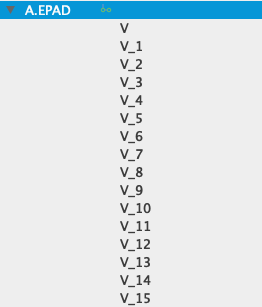 Connect all the pads to the same pin that the thermal pad represents
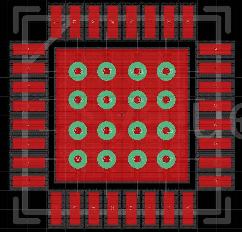 Pads with polygon on the top layer
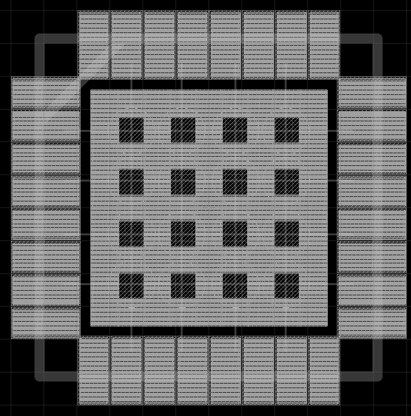 tStop layer
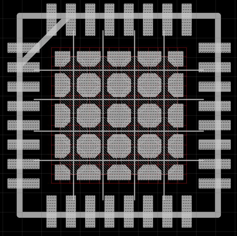 tCream layer